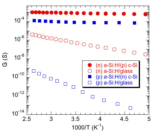
Figure 7.

Arrhenius plots of the planar conductance measured on various samples. Red circles for (n) a-Si:H, blue squares for (p) a-Si:H, full symbols for layers deposited on c-Si wafer (on opposite doping type with respect to the deposited a-Si:H layer), open symbols for layers deposited on glass.
