
Figure 1.
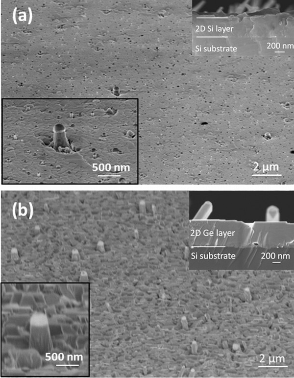
SEM images of Si NWs and Ge NWs. (a) Low-magnification SEM images of sample of Si NWs. The bottom inset shows a higher magnification of a Si NW. The top inset is a cross-sectional SEM image of the sample showing the substrate and the 2D Si layer on top of it. (b) Low-magnification SEM images of Ge NWs. The bottom inset shows a Ge NW. In the top inset, the cross section of the sample is shown, and the Si substrate, the 2D Ge layer, and some NWs are visible