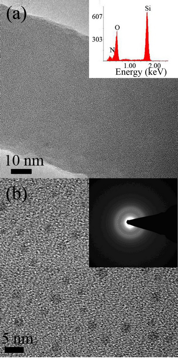
Figure 2.

TEM images of the surface and cross-section morphologies of a nanowire. (a) TEM image of a Si-O-N nanowire and the corresponding EDX analyses as an inset. (b) An HRTEM image of the nanowire's cross-section and the corresponding SAED patterns as an insert.
