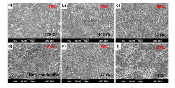
Figure 5.
SEM images of Ag NW films with different thickness. (a-c) SEM images of the surface of films with increasing thickness from NW sample 1# and (d-f) films made from NW sample 3#. The corresponding optical transmittances at 550 nm and sheet resistivity of thin films are indicated on the images: (a) 175 Ω/sq, T = 75%; (b) 102 Ω/sq, T = 66%; (c) 32 Ω/sq, T = 55%; (d) non-conductive, T = 63%; (e) 47 Ω/sq, T = 54%; (f) 11 Ω/sq, T = 37%.

