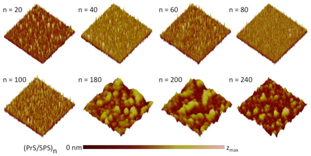
Figure 3. Surface morphology of (PrS/SPS)n PEMs surfaces.
AFM images (10 μm × 10 μm area) showed variation in the nanoscale topography of the surface of dry (PrS/SPS)n PEMs at different thicknesses (zmax = 110 nm, 60 nm, 30 nm, 35 nm, 40 nm, 1500 nm, 1600 nm, and 1000 nm for n = 20, 40, 60, 80, 100, 180, 200, and 240, respectively).

