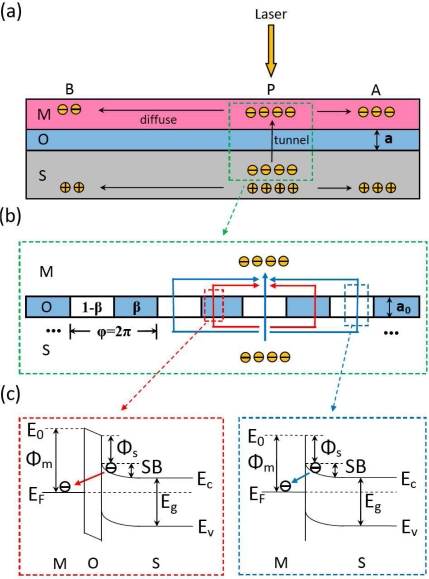
Figure 16.
Diagram of oxide thickness effect of LPE in MOS structure. (a) LPE mechanism in MOS structure with a fully covered oxide layer. (b) Electronic interference based on un-fully covered oxide layer when excited electrons transit from semiconductor to metal. The red (or blue) arrows represent the electrons tunneling through the walls (or passing through the windows) from semiconductor to metal. (c) Band models of electrons as tunneling through the walls (red part) and passing through the windows (blue part) from semiconductor to metal.

