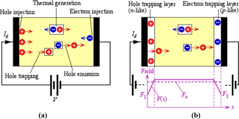
Figure 12.
(a) In a single layer of a-Se sandwiched between two electrodes, the dark current is due to the injection of holes (most dominant) and electrons from the positive and negative contacts respectively as well as some thermal generation of electron and hole pairs or hole emission from defect states. (b) In the case of an x-ray photoconductor, there are two thin layers between the a-Se and the electrodes. The hole-trapping layer traps holes and allows electron transport (an n-like layer) and the electron-trapping layer traps electrons and allows hole transport (a p-like layer). The structure is often referred to as an nip type a-Se photoconductor. The radiation receiving side is the positive electrode.

