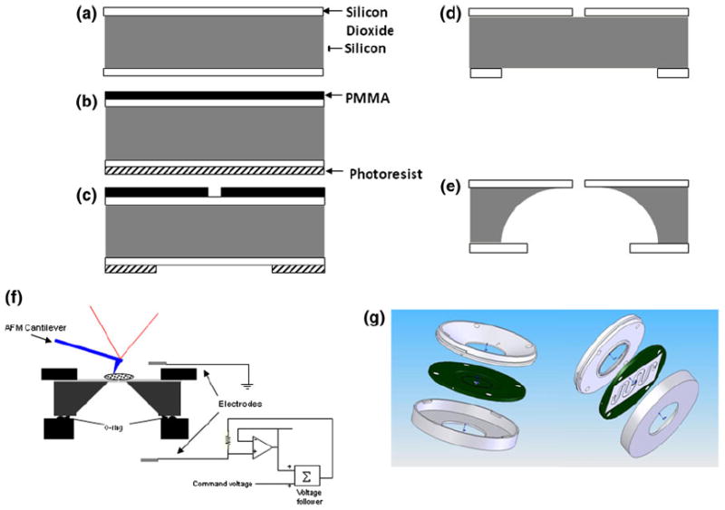
FIGURE 1.

Fabrication of the planar patch clamp chip, microfluidics chamber and integrated apparatus: (a) Oxidized silicon wafer was used as the starting material. (b) PMMA and photoresist were spin-coated on the top and the bottom, respectively. (c) 1 μm circles were defined in PMMA using electron beam lithography and circles of about 50 μm were defined, aligned to the top circles from the back of the wafer in the photoresist using photolithography. (d) Silicon dioxide was anisotropically etched using RIE; PMMA and photoresist were then removed. (e) Silicon was etched isotropically using a dry XeF2 based process. (f) Schematic cross-section of the liquid cell (not to scale). (g) SolidWorks drawing of the liquid cell.
