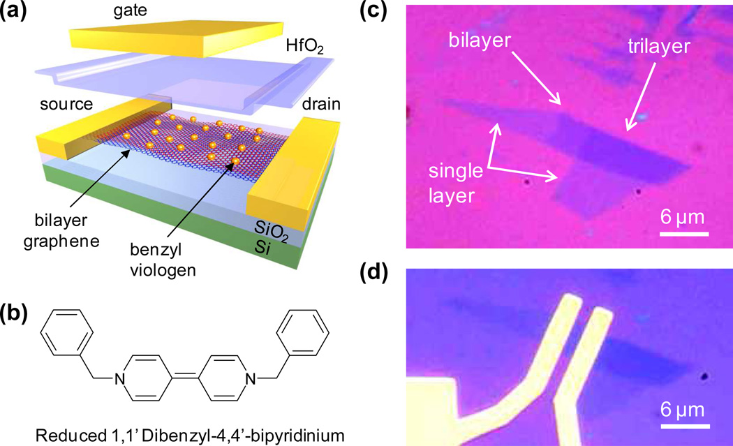
Figure 1.
(a) The schematic illustration of the benzyl viologen doped bilayer graphene dual-gate transistor. From top to bottom: top-gate electrode (Cr/Au), top-gate dielectric (50 nm HfO2), benzyl viologen doped bilayer graphene with source and drain electrodes (Cr/Au), 300 nm SiO2 bottom-gate oxide, and silicon bottom-gate. (b) Molecular structure of the reduced benzyl viologen molecule. (c) Optical microscopy images of an exfoliated graphene flake and (d) the corresponding bilayer graphene FET. The arrows in (c) indicate single layer, bilayer, and trilayer graphene sheets.

