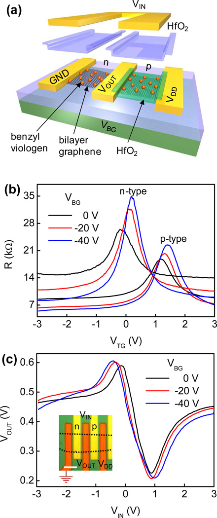
Figure 4.
(a) The schematic illustration of a complementary inverter. (b) The switching behavior of an n-type (BV doped) and a p-type (undoped) bilayer graphene FET as a function of top-gate voltage at different bottom-gate voltages. (c) The electrical switching characteristics (at various bottom-gate voltages) of a complementary inverter assembled by connecting an n- and a p-type bilayer graphene FET together. The inset shows an optical image of a complementary bilayer graphene inverter. Scale bar is 5µm.

