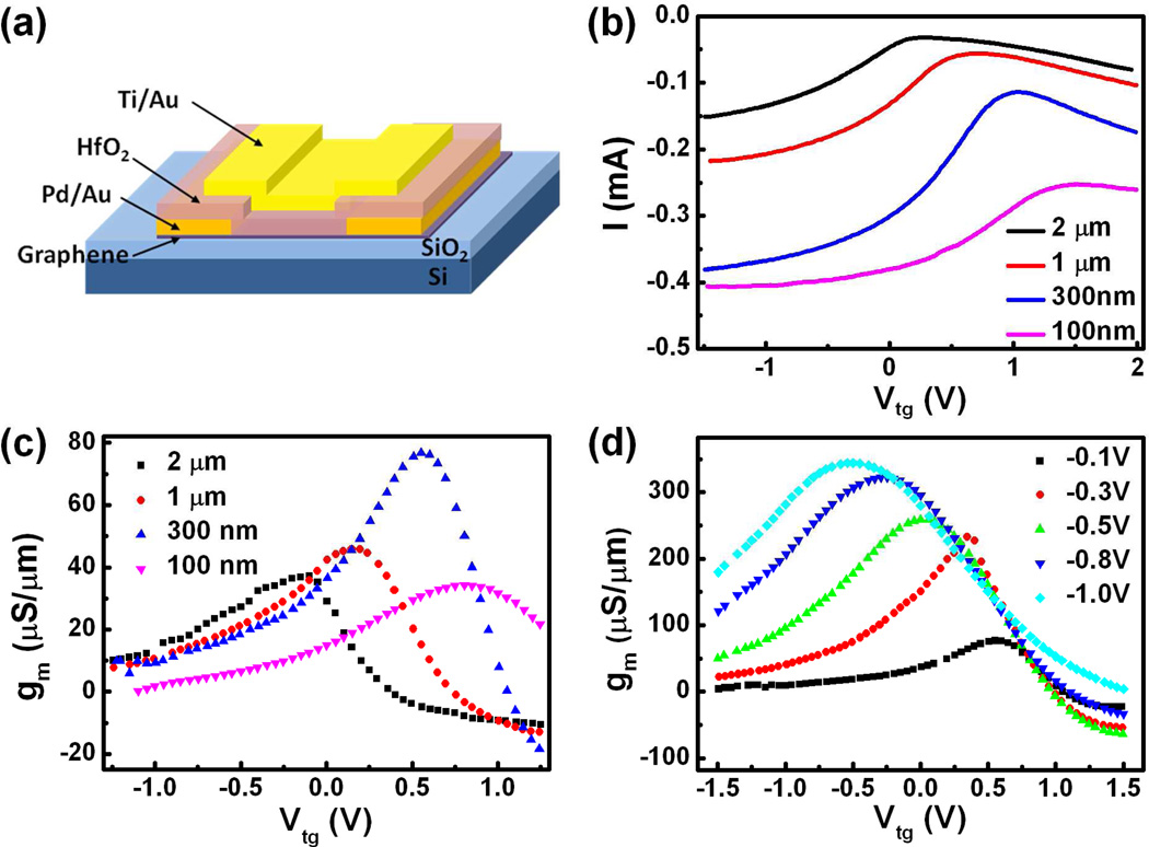
Figure 1.
(a) Schematic illustration of the device structure of top gated graphene transistors for the evaluation of the channel length scaling effect. (b) Transfer characteristics of top-gated graphene transistor at Vds=−0.1V with channel lengths 2 µm, 1 µm, 300 nm and 100 nm. The channel width is 3.4 µm for all devices. (c) The corresponding transconductance of the devices shown in (b) at Vds=−0.1V. (d) The evolution of transconductance with gate voltage for the 300 nm channel device at bias voltage −0.1V, −0.3V, −0.5V, −0.8V and −1.0V.

