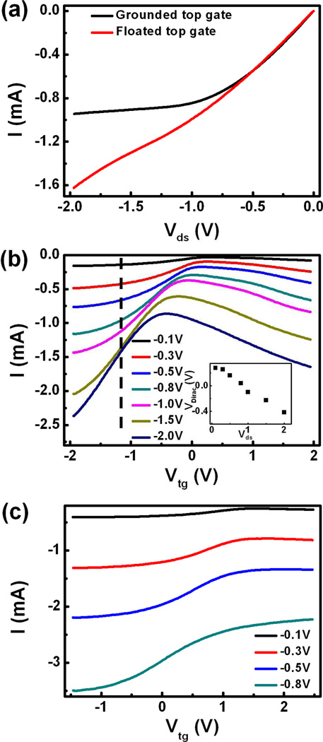
Figure 3.
(a) I–V characteristic of a long channel device (L=5.6 µm) under grounded or floated gate condition. (b) Transfer characteristic at different bias voltage for the device with L=2 µm. The inset shows Dirac point shift as a function of bias voltage. (c) Transfer characteristic at different bias voltage for the device with L=100 nm.

