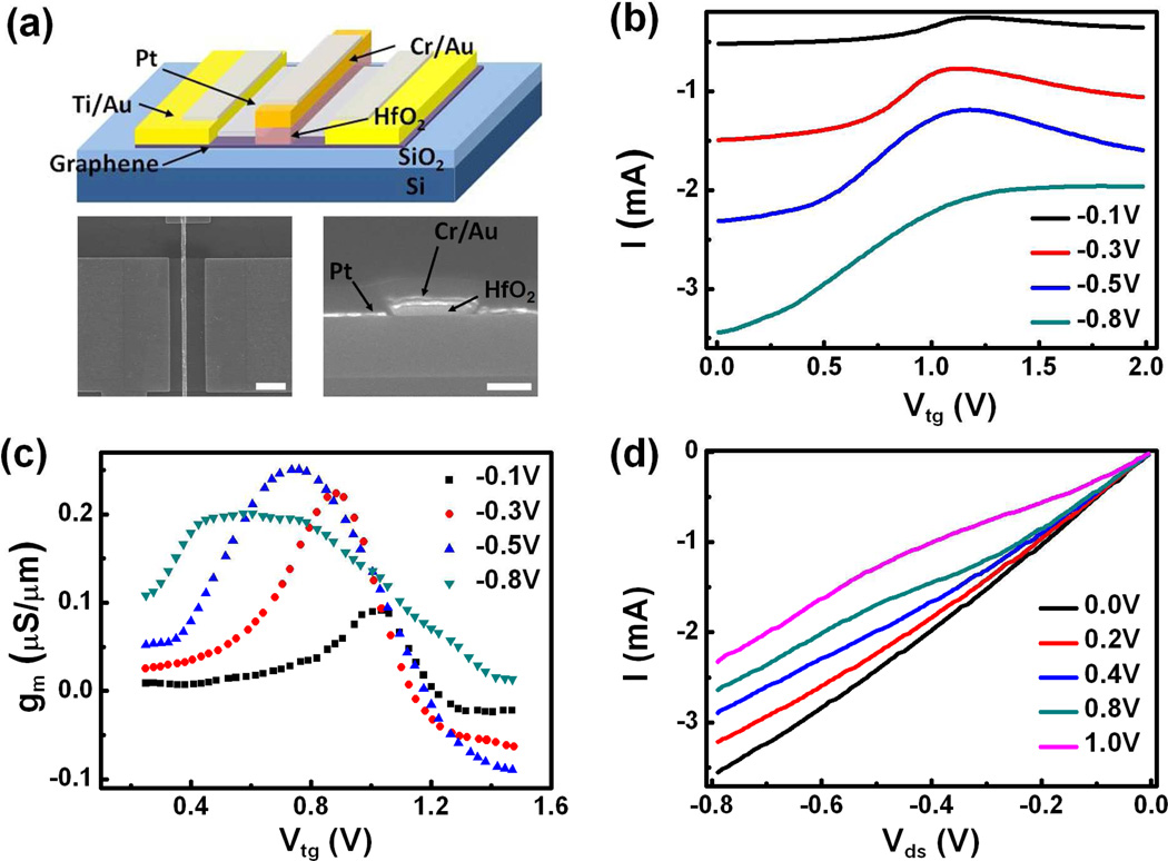
Figure 4.
(a) Schematic (top), top view (bottom left) and cross section (bottom right) SEM image of a typical self-aligned device. The scale bar indicates 2 µm in the top view SEM image, and 200nm in the cross section SEM image. (b) Transfer characteristic and (c) corresponding transconductance under different bias voltage for an L=300 nm self-aligned device. (d) Output characteristics of the same device.

