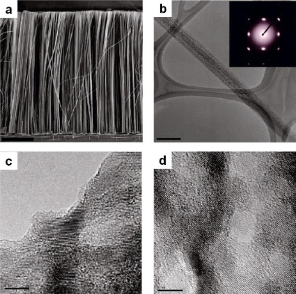
Fig. 1.

Structural characterization of the porous silicon nanowires synthesized from highly doped p-type Si wafers (0.005 Ω·cm). (a) SEM image of the cross section of the as-etched porous silicon nanowires. (b) TEM image of a typical porous silicon nanowire from which the SAED 15 (inset) pattern was obtained. (c, d) Phase contrast TEM images of the silicon lattice around pores near the surface and in the interior of the nanowire. The scale bar is 10 μm for a, 200 nm for b, and 5 nm for c and d. (Adapted from ref. 43. Copyright 2009 American Chemical Society.)
