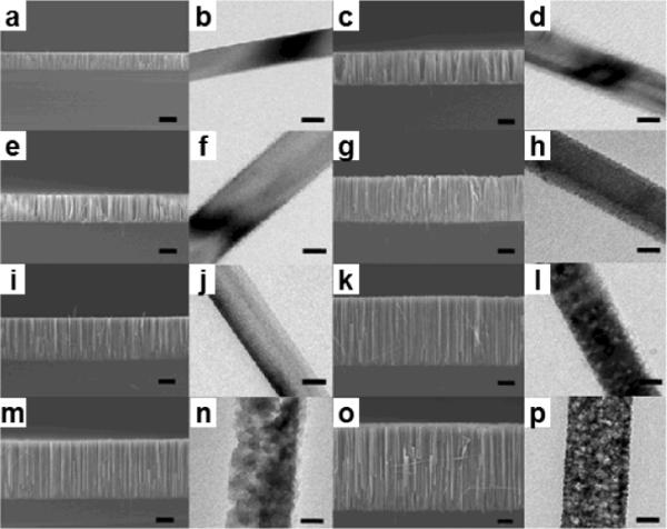
Fig. 2.

SEM and TEM images of silicon nanowire morphology from n-Si(100) with 0.008–0.02 Ω·cm resistivity in etchant solutions composed of 4.8 M HF and variable concentrations of H2O2 through a two-step reaction. (a,b) 0.1 M H2O2 for 30 min; (c,d) 0.1 M H2O2 for 60 min; (e,f) 0.15 M H2O2 for 30 min; (g,h) 0.15 M H2O2 for 60 min; (i,j) 0.2 M H2O2 for 30 min; (k,l) 0.2 M H2O2 for 60 min; (m,n) 0.3 M H2O2 for 30 min; and (o,p) 0.3 M H2O2 for 60 min. The scale bars for all SEM and TEM images is 10 μm and 60 nm, respectively. (Adapted from ref. 42. Copyright 2009 American Chemical Society.)
