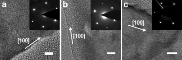
Fig. 3.

High-resolution TEM images with SAED patterns of nonporous and porous silicon nanowires. (a) Nanowires obtained from the reaction in 0.1 M H2O2 and 4.8 M HF for 30 min. (b) Nanowires obtained from the reaction in 0.2 M H2O2 and 4.8 M HF for 30 min. (c) Nanowires obtained from the reaction in 0.3 M H2O2 and 4.8 M HF for 60 min. All the scale bars are 5 nm. (Adapted from ref. 42. Copyright 2009 American Chemical Society.)
