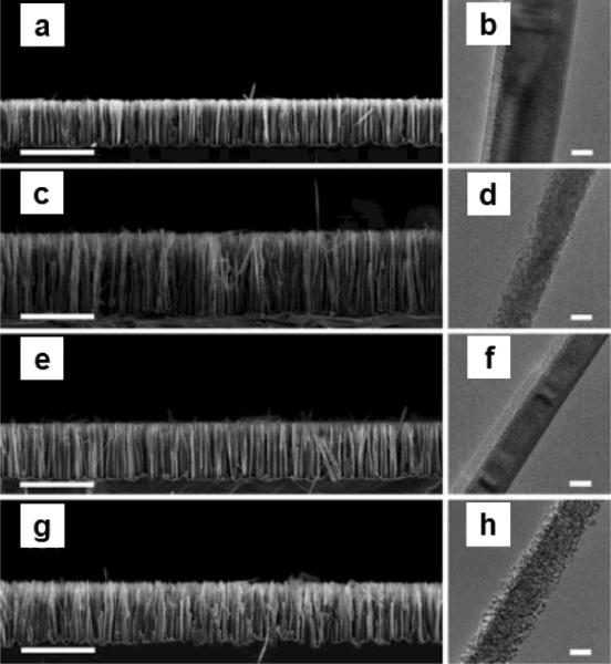
Fig. 4.

SEM and TEM images porous silicon nanowires etched from n-Si (100) with a resistivity of 1–10 Ω cm at different temperature, time and H2O2 concentrations. (a, b) 0 M H2O2, 60 min, 60 °C; (c, d) 0.3 M H2O2, 60 min, 60 °C; (e, f) 0 M H2O2, 40 min, 80 °C; (g, h) 0.3 M H2O2, 40 min, 80 °C. Scale bars for SEM and TEM images are 10 μm and 50 nm. (Adapted from ref. 47. Copyright 2011 Royal Chemical Society.)
