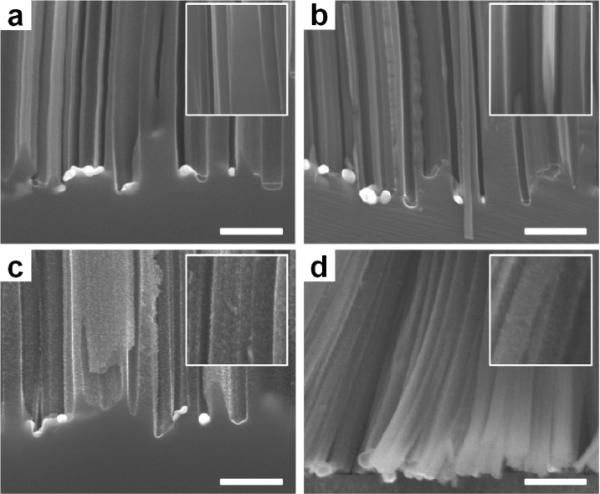
Fig. 6.

Cross-sectional SEM images of silicon nanowires etched from four n-type wafers with various resistivities for 15 min in the etchant solutions containing 0.3 M H2O2 with nitric acid treatment. (a) 1–5 Ω · cm; (b) 0.3–0.8 Ω · cm; (c) 0.008–0.016 Ω · cm; and (d) 0.001–0.002 Ω · cm. Scale bars is 500 nm. (Adapted from ref. 46. Copyright 2011 American Chemical Society.)
