Figure 3.
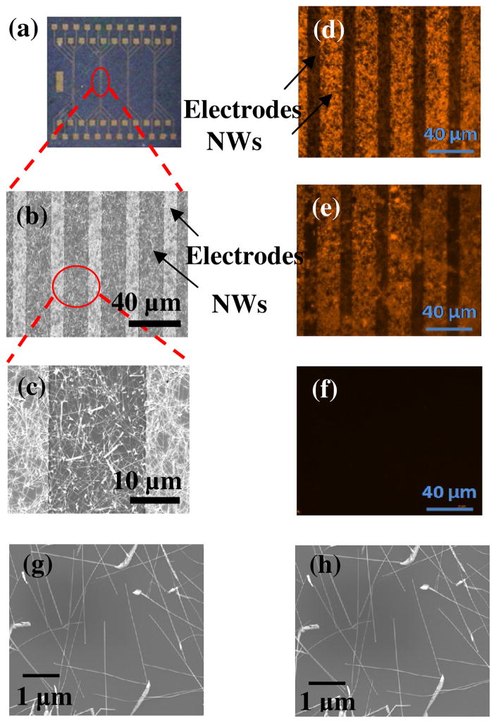
(a) An optical image of In2O3 NW mats with four groups of electrode deposited on top. (b) A typical SEM image taken in the center region of one group of electrodes. (c) The same image at higher magnification. Figure (d)–(f) are fluorescence images of In2O3 NWs near three groups of electrodes. NWs were first functionalized with DMP-PA. An oxidizing potential of 950 mV was applied to the first group (d), converting the DMP-PA coating to BQ-PA. The second group (e) was subjected to an oxidizing potential of 950 mV, followed by a reducing potential of −80 mV, converting the DMP-PA coating to a HQ-PA. The third group (f) has the original DMP-PA coating. The three groups were treated with thiolated single strand DNA, and then its complementary DNA labeled with a fluorescent dye. After extensive rinsing with PBS buffer, the NWs near the three groups of electrodes were examined under fluorescent microscope. Figure (g) and (h) are SEM images of the same area of a NW mat sample before and after DMP-PA coating, respectively. The size and length of NWs didn’t change after the coating.

