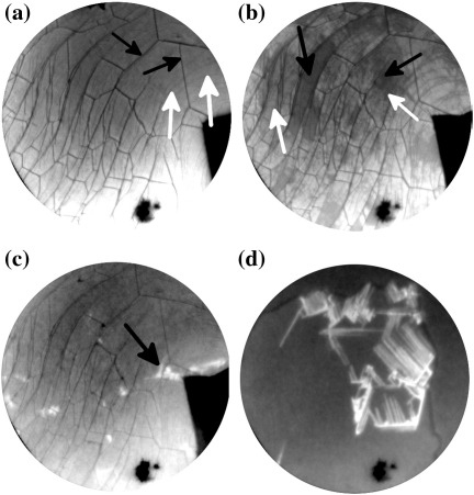
Fig. 1.
LEEM images acquired at a temperature of 320 K with an electron energy of 2.7 eV for (a)–(c) and 3.7 eV for (d). The Field of View (FoV) is 6 μm for (a)–(c) and 4 μm for (d). Times indicated are measured with respect to the start of 6P deposition. (a, t = 0 s) A single graphene flake on the Ir{111} surface is imaged prior to exposure to 6P. Graphene wrinkles (indicated with black arrows) and the faint contours of Ir{111} surface steps (indicated with white arrows) are visible on the single layer graphene flake. (b, t = 813 s, 0.52 6P/nm2) The graphene flake is covered by a wetting layer of 6P. The two additional grey levels correspond to the initial layer formed by flat lying face-on molecules only (white arrows), and the final wetting layer with a face-on/edge-on, like structure (black arrows). The nucleation of this film happens next to the wrinkles. (c, t = 1268 s, 0.80 6P/nm2) Bright crystallites occur on top of the wetting layer next to the wrinkles (black arrow). (d, t = 2149 s, 1.36 6P/nm2) Parallel needles continue to grow with ongoing deposition. The dark area in the lower part of the images is a defect in the channel plate.

