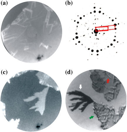
Fig. 5.
(a, t = 2130 s, 1.35 6P/nm2) 10 μm FoV LEEM image acquired at an electron energy of 2.7 eV and 352 K. A single graphene flake on the Ir{111} surface is imaged after deposition of 6P. The edge of the graphene flake is visible in the upper left part. The graphene flake is covered with 6P needles of different orientation. (b) μLEED pattern measured from graphene covered by the wetting layer at an electron energy of 19.3 eV. (c) 20 μm FoV LEEM images acquired at an electron energy of 2.7 eV and a temperature of 352 K. The Ir{111} surface with an irregular shaped island and three graphene flakes covered with 6P is visible. The 6P island on the Ir{111} surface is connected to the graphene flake. (d) 50 μm FoV PEEM image acquired after stopping the 6P deposition. 6P needles, graphene flakes, and 6P islands on Ir are present and marked by red, green, and white arrows, respectively (352 K).

