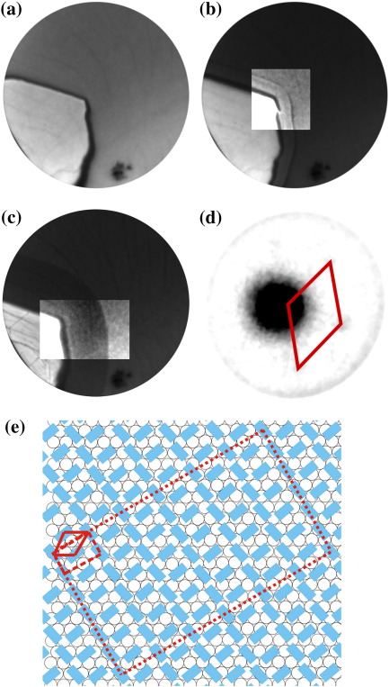
Fig. 7.
6 μm FoV LEEM images acquired at an electron energy of 2.7 eV and temperature of 405 K. (a, t = 0 s) A graphene flake residing on the Ir{111} surface prior to exposure to 6P. Wrinkles and the contours of Ir{111} surface steps are visible on the single layer graphene flake. (b, t = 831 s, 0.53 6P/nm2) The nucleation of a 6P film takes place on the edges of the graphene flake, as is witnessed by the appearance of a band of different intensity at the edge of the graphene (see contrast enhanced center). The reflected intensity from the Ir{111} surface decreases. Three different levels of contrast are found. From left to right: graphene, ordered 6P layer and 6P lattice gas on Ir{111}. (c, t = 1391 s, 0.88 6P/nm2) The ordered 6P film extending from the graphene flake has grown further (see contrast enhanced center). (d) A μLEED pattern is measured at electron energy of 25.6 eV using a 1.4 μm field-limiting aperture from the Ir{111} surface area completely covered with the ordered 6P layer. The nearest neighbor cell is highlighted by red lines. (e) The structural model proposed from the μLEED pattern shown in panel (d). The molecules are arranged in an up-right standing orientation on Ir{111}. The unit cell (dashed lines) and the nearest neighbor cell (solid line) are shown. The 6×6 superstructure is indicated by a dotted line. Times indicated are measured with respect to the start of 6P deposition.

