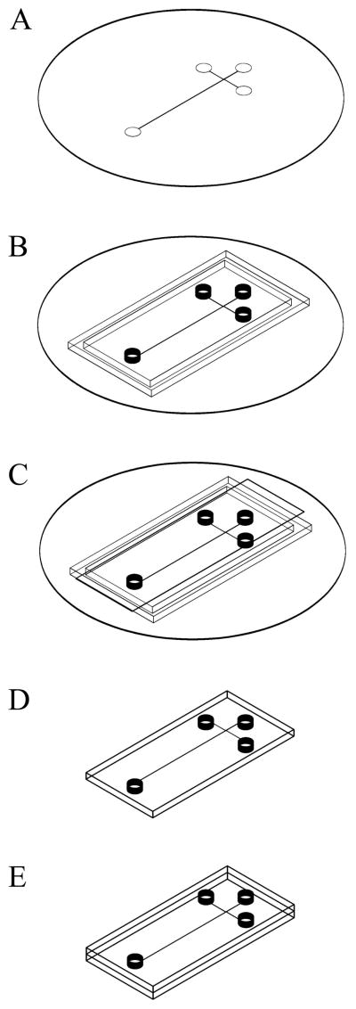
Figure 1.
Schematic showing the procedure used for the fabrication of TPE microfluidic devices. (A) A SU-8 patterned silicon master is treated with HMDS vapor. (B) A PDMS mold surround and posts are placed on the master. (C) TPE resin containing UV photoinitiator and catalyst is poured into the master assembly; transparency film is used on the top. (D) Following exposure to UV radiation, the semicured TPE replicas are removed from the master, and (E) brought into contact. Additional UV exposure and heat are used to completely cure the TPE chip.

