
Figure 3.
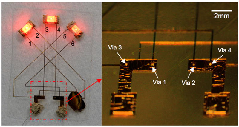
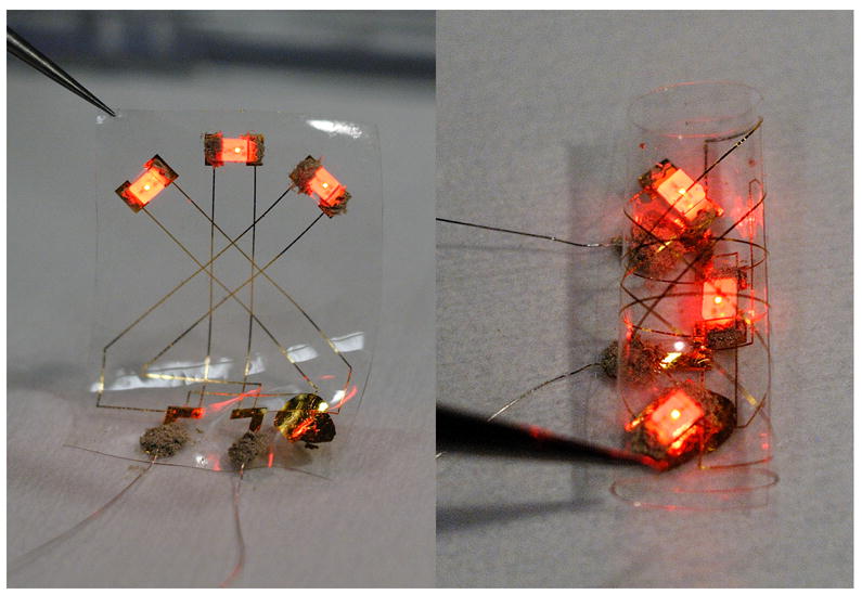
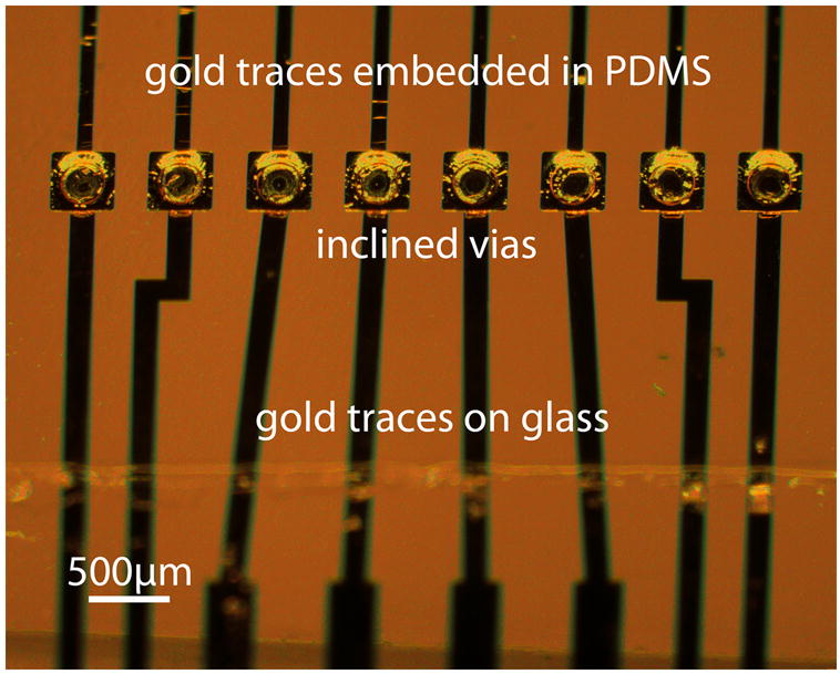
Demonstration of multilayer interconnects within PDMS and between PDMS and a rigid substrate. (a) A prototype device with three interconnected conducting layers. The total thickness of this device is 100μm, which includes a 70μm PDMS base layer and three 10μm PDMS insulation layers. The thin gold lines on different conducting layers are all 100μm wide. Three LEDs were glued using conductive polymer (Silicone Solutions; Twinsburg, OH) to their exposed contact pads on separate conducting layers. Power was supplied to the device through two silver wires glued to the contact pads on the bottom conducting layer. Traces 1 and 2 and power lines are on the bottom conducting layer; Traces 3 and 4 are on the middle conducting layer, and interconnected to the power lines through Vias 1 and 2, respectively; Traces 5 and 6 are on the top conducting layer, and interconnected to the power lines through Vias 3 and 4, respectively. Vias 3 and 4, both formed by two stacked inclined vias during two rounds of processes, go through two PDMS insulation layers, and thus are deeper than Vias 1 and 2. (b) Deformation of the device in (a). The device was scrolled into a roll while still maintaining its electrical functionality (right). (c) Via bonds on a rigid substrate (glass). Gold traces embedded in PDMS are interconnected to gold traces on glass through inclined vias. Only the bonding area is shown in this figure. In this area, PDMS was cured on bare glass. This formed a strong bonding between PDMS and the glass substrate.