Figure 4.
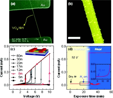
(a) Scanning electron microscopy (SEM) image of an individual VO2 nanowire device configured with appropriate Ohmic contacts for electrical measurements in a gaseous atmosphere. (b) SEM image of a Pd-decorated VO2 nanowire. The Pd particles, 5–22 nm in diameter, are noncontinuous and cover the surface of the nanowire uniformly (scale bar, 200 nm). (c) I–V curves obtained at 50 °C for Pd-decorated VO2 nanowire after various exposure times to hydrogen gas (5 sccm), added to the background argon stream (10 sccm). (d) The change in current for a Pd-decorated VO2 nanowire biased at 10 V as a function of time of exposure to hydrogen gas. Initially the current increases gradually with hydrogen exposure time and then at ∼7 min increases dramatically by ∼3 orders of magnitude (5 × 10⁻⁶ A → 6 × 10⁻³ A) in the absence of the series resistor (Reprinted from reference [24] with permission from American Chemical Society).

