Fig. 2.
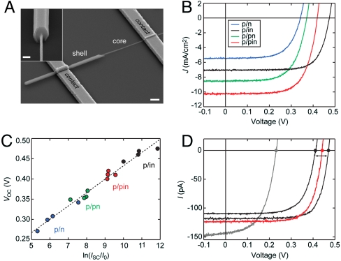
Transport properties of single-NW solar cells. (A) SEM image of a standalone NW device with lithographically defined Ti/Pd contacts overlapping the shell and core regions of the NW; scale bar, 1 μm. Inset: SEM image of a single core/shell NW transferred onto a Si3N4 substrate and wet-chemically etched on the lower portion to reveal the core; scale bar, 200 nm. (B) Current density-voltage (J - V) characteristics of single-NW solar cells composed of four distinct diode geometries (refer to Fig. 1A). (C) Open-circuit voltage (VOC) versus the logarithm of the ratio of short-circuit current (ISC) to dark saturation current (I0) for the four best devices from each diode geometry. A fit (dashed line) to the ideal diode equation yields an ideality factor n = 1.28. This value is lower than those calculated from dark I - V data for individual devices, although we note that our values for n (1.3–1.8) indicate consistently the presence of carrier recombination within the depletion region of all devices. (D) Current-voltage characteristic (red) for a p/in NW device for which Au catalyst was removed by aqueous KI/I2 wet-chemical etch prior to shell growth. Gray curve is for an i/pin Si NW device whose growth was catalyzed by Al. Black curves show current-voltage characteristics for a single Au-catalyzed p/in NW device measured before and after oxidation of its surface in air for one week.

