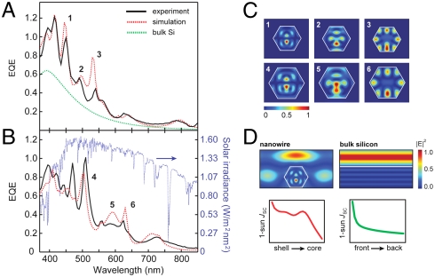
Fig. 3.
Enhanced and tunable absorption in NWs. (A) External quantum efficiency (EQE) as a function of wavelength for a p/in NW (black curve) and simulated EQE spectrum (dashed red curve) produced with no adjustable parameter other than the size of the NW (height of 240 nm). Dashed green curve shows the simulated spectrum for top 240 nm of planar bulk Si. (B) EQE spectrum (black curve) of a p/pin NW compared to the irradiance of the AM1.5G solar spectrum (dashed blue curve). Dashed red curve corresponds to simulated EQE calculated with no other adjustable parameter besides the NW size (height of 305 nm). (C) FDTD simulations of resonant mode spatial profiles for p/in (profiles 1–3) and p/pin (profiles 4–6) structures. Labeled profiles correspond to the EQE peaks labeled identically within Fig. 3 A–B and profiles in each column correspond to the same mode excited within both structures. All profiles are for TM polarizations and use a linear color scale representing absorption (not electric field intensity) within the mesoscopic structures. Resonant modes labeled 3 and 6 correspond to whispering-gallery type modes while all others correspond to Fabry–Perot resonances. (D) Plot of electric field intensity for plane wave (λ = 445 nm) interacting with a NW (Left) and bulk Si (Right). White line defines outline of NW and top surface of bulk Si. Beneath are plots of total JSC as a function of position inside the NW or bulk Si.

