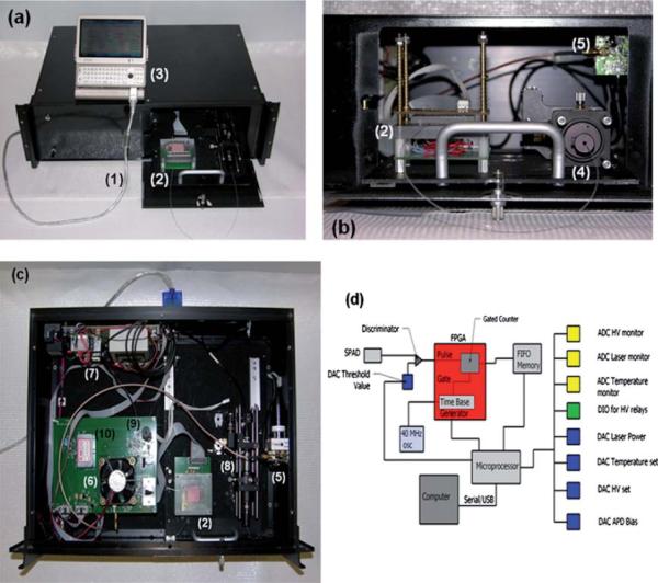
Fig. 1.

(a) Picture of the compact SMD instrument connected to a mini-computer for data collection and instrument control. (b) Access panel for loading sample into the microfluidic chip and connecting the collection fiber optic to the fiber U-bench, which contained optical fibers and another optical fiber interfaced to the SPAD. (c) Inside the compact SMD instrument showing the arrangement of the VCSEL, SPAD, FPGA and other peripheral electronics. (d) Schematic of the FPGA that was used for data acquisition and single-photon processing. The FPGA counted signals from the SPAD and output information to the first-in first-out (FIFO) memory. (1)–USB interface cable to the controlling computer; (2)–microfluidic chip sitting atop a mounting stage, which is accessed through a drawer that slides out from the main instrument case; (3)–controlling computer; (4)–fiber bench with optical cable connected to the fluidic chip; (5)–SPAD with integrated fiber optic; (6)–cooling fan for the FPGA, which is located underneath this fan; (7)–various power supplies; (8)–fiber bench with optical filters; (9)–VCSEL with integrated fiber; and (10)–electrophoresis power supply to actuate fluids electronkinetically.
