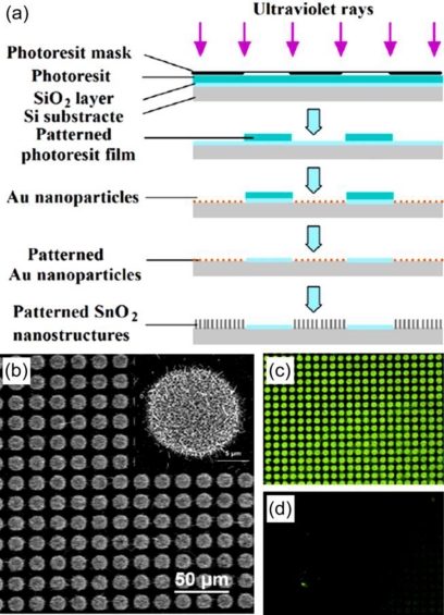
Figure 1.
(a) Schematic illustration of the fabrication of patterned SnO2 nanomaterials on silicon substrate. (b) Low- and high- magnification (insert) SEM images of the patterned SnO2 nanomaterials. The fluorescence emission photos from (c) covalent- and (d) noncovalent-linked probe DNA. Reprinted with permission from [43]. Copyright (2008) IOP Publishing Ltd.

