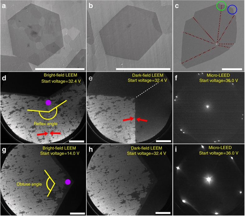
Figure 1. Characterization of graphene grains grown on Pt substrates.
(a,b) Scanning electron microscope (SEM) images of two hexagonal graphene grains on a polycrystalline Pt foil, which were grown with 4 sccm CH4 and 700 sccm H2 at 1,040 °C for 180 min. The scale bar in (a) is 1 mm, and in (b) is 0.5 mm. (c) SEM image of an irregular graphene, which contains several grains, on a single-crystal Pt(111). It was grown with 4 sccm CH4 and 700 sccm H2 at 1,040 °C for 45 min. The red dashed lines indicate the grain boundaries determined by LEEM and micro-LEED patterns. The scale bar is 100 μm. (d,e) Bright-field and dark-field LEEM images recorded at the region with a reflex angle in the green circle in (c). A clear boundary indicated by an arrow was observed in the bright-field LEEM image, and the two sides of this line show sharp contrast in the dark-field LEEM images. The scale bars in (d) and (e) are 10 μm. (f) Micro-LEED pattern taken from the region indicated by a purple dot in (d), showing two spot patterns. (g,h) Bright-field and dark-field LEEM images recorded at the region with an obtuse angle in the blue circle in (c), showing no obvious difference through the whole region, without boundaries being observed. The scale bars in (g) and (h) are 10 μm. (i) Micro-LEED pattern taken from the region indicated by a purple dot in (g), showing only one pattern. For details about the black bubble-like regions in (d–h), see Supplementary Fig. S5.

