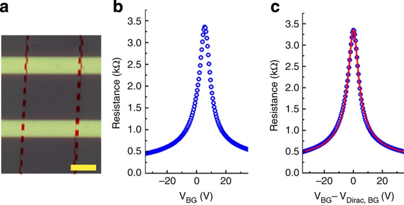
Figure 6. Transport property of single-crystal graphene transferred from Pt to a Si/SiO2 substrate.
(a) Optical image of a back-gate graphene field-effect transistor. The scale bar is 5 μm. (b) Device resistance versus back-gate voltage (VBG) of this graphene field-effect transistor. (c) Device resistance versus VBG−VDirac, BG (VBG at the Dirac point) and with a model fit (solid red line).

