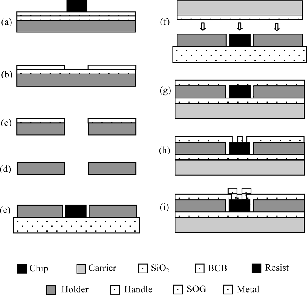
Fig. 2.
VCSIT process steps to package a chip. (a) Chip is placed on the resist-coated, oxidized silicon holder. (b) A hole with the same size as the chip is patterned in the resist using the chip as photomask. (c) The pattern is transferred to the oxide layer, and through-holder etch is performed (d) Oxide on the holder is removed. (e) The holder and the chip are placed face-down on a handle substrate. (f) The BCB-coated carrier is bonded with the backside of the chip and the holder. (g) The gap between the chip and the holder is filled and the top surface is planarized with SOG. (h) Vias to the contact pads of the chip are created. (i) Metal interconnects from the chip to the holder are patterned.

