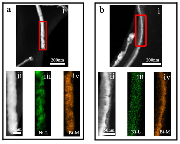
Figure 4.
Images of a Bi-Ni nanowire (a) and nanocable (b) obtained using STEM. STEM HAADF images of (i) a Bi-Ni nanowire and nanocable and (ii) after an EDS image scan of the marked area in (i). Elemental mapping of the (iii) nickel and (iv) bismuth X-ray intensities compositing along the nanowire and nanocable.

