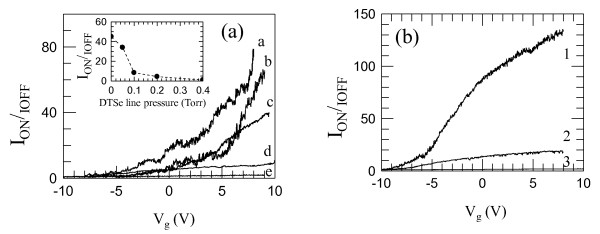
Figure 5.
On/off current ratio Ion/Ioff as a function of the gate bias. Panel (a) refers to the investigated set of samples a, b, c, d, and e. Inset: maximum value of the on/off current ratio plotted as a function of the DtBSe precursor line pressure. Panel (b) was measured for FET devices having identical growth conditions and geometries of sample c with gate-to-nanowire distances of 290 (curve 3), 125 (curve 2), and 70 nm (curve 1), respectively.

