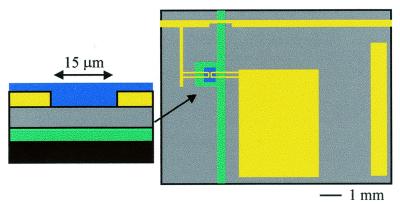
Figure 2.
Schematic illustration of the cross section of a display transistor and layout of a unit cell (blue, semiconductor; yellow, gold source/drain level; gray, dielectric; green, gate level; black, substrate). Each transistor controls the switching of electronic ink that lies above a pixel electrode that is electrically connected to the drain side of the transistor. The rectangle of gold on the right is generated by a raised support feature on the stamp that prevents mechanical sagging in the recessed regions during printing.

