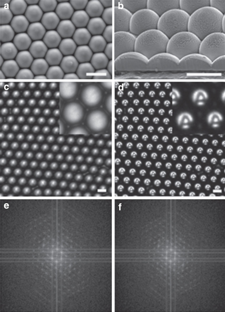
Figure 2. Morphology and optical properties of the CaCO3 microlens array.
(a) SEM image of the homogeneous and well-ordered CaCO3 microlens array from top view. (b) SEM image of cross-sectioned microlens array from 52° tilted view. The microlens array was etched by using focused ion beam with Ga ion beam. The bright layer on the surface of the microlens is the Pt coating, the surface without Pt coating was damaged by the ion beam and shows roughness as a result. The microlens structures were connected with each other. (c,d) Optical microscopy images of CaCO3 microlens array and inversely projected 'A' array, respectively. The magnified images are shown in each inset. (e,f) The Fourier transformed images from c and d, respectively. All the scale bars are 5 μm.

