FIG. 1.
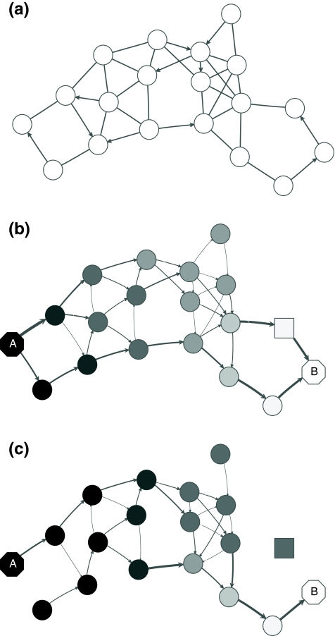
Absorbing mode formalism can be extended beyond resistor networks. Consider, for example, the directed graph shown in (a), where all edges, directed and undirected have weight 1. This graph can be modeled as a resistor network by treating all edges as undirected (b). Applying a unit voltage at node A and grounding at node B leads to the current flowing from A to B. The voltage at each node is indicated by shading (dark means high voltage) while the current at each edge is indicated by the thickness and the direction of the arrow corresponding to that edge. The equivalents of voltage and current can be obtained for the original graph using the absorbing mode with the same boundary (c). Note the qualitative difference between the results in (b) and (c): the node shaped as square conducts significant current in (b) but is totally isolated in (c).

