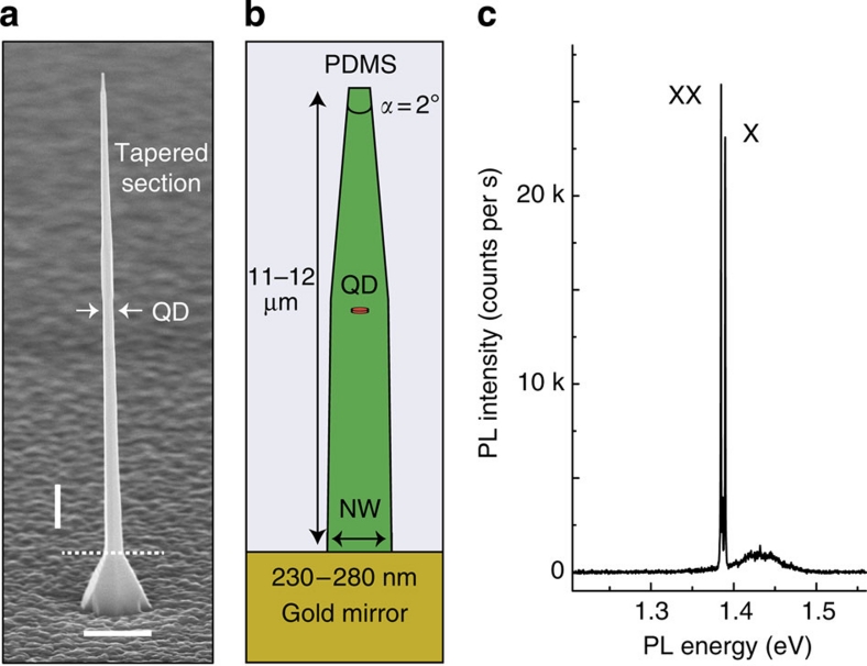
Figure 1. Tailored nanowire waveguide geometry.
(a) SEM image of tapered InP nanowire waveguide containing a single InAsP quantum dot (QD). The tapering angle of the nanowire is α=2° The nanowire breaks at the dotted line after transfer into PDMS. Vertical and horizontal scale bar: 1 μm. (b) Tailored nanowire geometry embedded in PDMS with bottom gold mirror. QD is indicated by the red dot and, by design, is positioned on the nanowire (NW) waveguide axis, where the emission is efficiently coupled to the fundamental waveguide mode. (c) Typical single dot PL of exciton (X) and biexciton (XX) in an individual tapered nanowire waveguide, exhibiting a clean optical spectrum over a large energy range. The broad peak at 1.43 eV originates from the InP nanowire.

