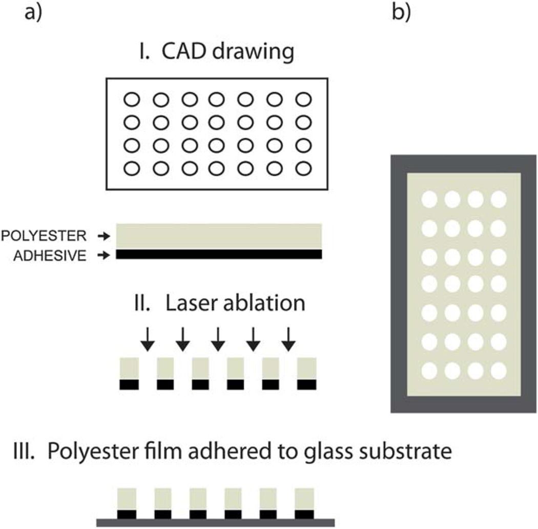
Fig. 1.
Schematic of the polyester microwell device fabrication process. (a) Fabrication steps: a drawing is generated in a CAD program (I) and used as a pattern for laser ablation of the polyester film (II). Finally, the patterned film is adhered onto a glass substrate through an adhesive side (III). (b) Top view of the device.

