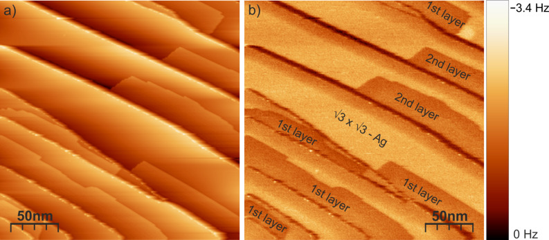
Figure 1.
(a) STM image of the PTCDA/Ag/Si(111) √3 × √3 surface. Scan area: 250 nm × 250 nm, tunneling voltage U = 0.9 V, tunneling current I = 70 pA. (b) Simultaneously recorded frequency shift at an oscillation amplitude of 2.8 Å. The Ag/Si(111) √3 × √3 surface gives rise to a larger frequency shift than the PTCDA islands.

