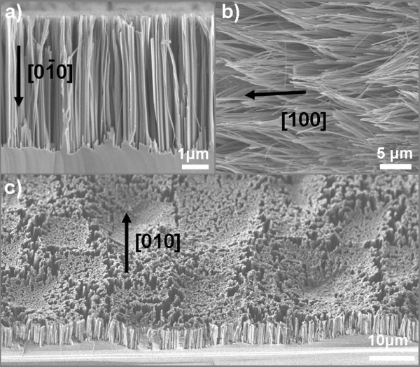
Figure 2.
SEM images of SiNWs grown along the three equivalent crystallographic orientations. SiNWs on different (100)-equivalent crystallographic orientations: (a) front side of the wafer, (b) wafer edges, and (c) back side of the wafer. The backside wafer surface is rough, and this roughness is reproduced on the SiNW surface since the NW length stays constant all along the surface.

