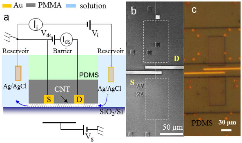
Figure 1.

(a) Schematic of the device structure of a combined SWCNT field effect transistor and nanopore device. The electrical measurement configuration for both electronic current and ionic current measurement is also shown. The distances between source (S) and drain (D) electrodes is 15μm and the barrier width is 30μm. (b) Scanning electron microscope (SEM) image of a used device after stripping off the covering PMMA layer. The two rectangles enclosed by white dash lines indicate the location of reservoirs. In the barrier region, one SWCNT bridges two reservoirs and is also contacted by both the source and drain electrodes. (c) Optical microscope image of a working device during measurement. The device is covered by a PDMS stamp with microfluidic channels and aqueous solution fills the reservoirs.
