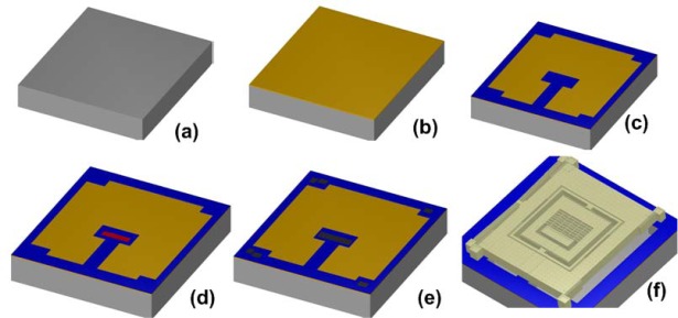
Figure 10.
Process flow for the fabrication of microgyroscope using MetalMUMPs in MEMSPro (a) N-type 〈100〉 silicon wafer (b) 2 μm thick isolation oxide layer (c) patterning of 0.35 μm thick silicon nitride layers (d) patterning of 0.7 μm thick Polysilicon layer (e) patterning of anchor metal layer (f) patterning of 20 μm electroplated structural layer of Ni and trench etch in the substrate.

