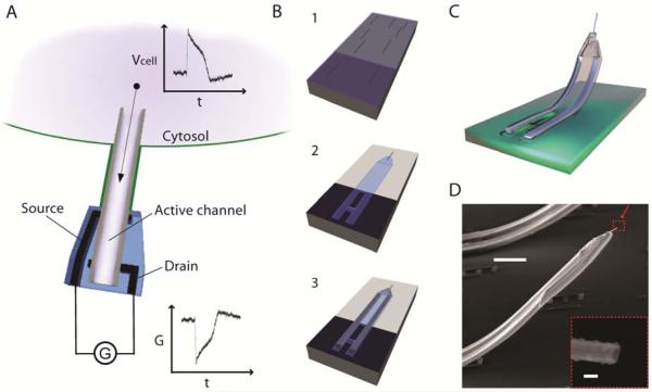
Figure 1. Principle and fabrication of the ANTT probe.
(A) Schematic view of an ANTT probe inserted into a cell and recording an intracellular action potential (Vcell vs. time, t) as a conductance (G) change in the active FET region between S/D contacts. Sensitivity to voltage changes from the external extracellular environment is effectively eliminated by SU-8 passivation of the nanotube region around the S/D contacts. The nanotube is shown as a half-cylinder for clarity. (B) Overview of the steps used for ANTT probe fabrication:14 (1) Transfer of Ge/Si core/shell nanowires (Ge/Si NWs) to a SU-8 layer that was deposited and prebaked on a sacrificial layer (colored silver). (2) Registration of positions of Ge/Si NWs and definition of the bottom SU-8 layer. (3) Definition of S/D metal contacts followed by the top SU-8 passivation layer. Final etching of the sacrificial layer and Ge NW core yields the Si ANTT probe. (C) Schematic of the completed ANTT probe following release from the substrate. (D) Scanning electron microscopy (SEM) image of an ANTT probe. Scale bar, 10 μm. Inset, zoom of the probe tip from the dashed red box. Scale bar, 100 nm.

