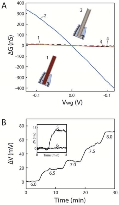
Figure 2. Potential and chemical sensitivities of ANTT devices.
(A) Change of conductance, ΔG, versus water-gate potential, Vwg, prior to (1) and after (2) H2O2 etching of the Ge NW core.14 Plots (3) and (4) correspond to ΔG versus Vwg for a Si/Si intrinsic-core/p-shell NW device before and after, respectively, etching using the same conditions as for the Ge/Si NW structure. All measurements were made in 1× phosphate-buffered saline (1×PBS) with a Ag/AgCl reference gate electrode. Insets, schematics of an ANTT device prior to (1) and after (2) H2O2 etching of the Ge NW core (colored deep red). (B) Change in potential, ΔV, in response to step changes in solution pH. The potential values were calculated from the measured ANTT device conductance using the measured water-gate sensitivity of 2.0 μS/V. Inset, ΔV as the pH is increased stepwise from 7.0 to 8.0 for an ANTT device (5) and the same device after closing the tip with SU-8 resist to prevent solution access (6).

