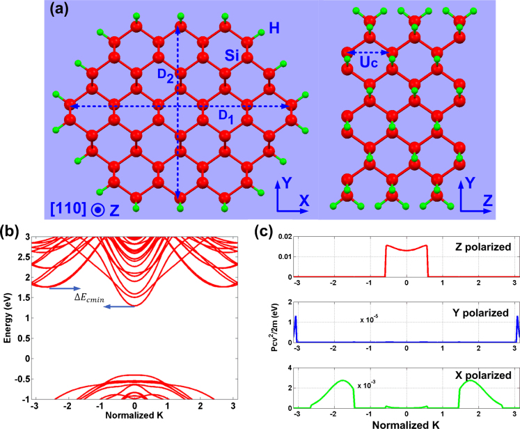
Figure 1. Cross section, electronic structure and momentum matrix element.
(a: left) Cross section of a [110] SiNW with the diameter (d) of 1.7 nm in xy plane. Diameter (d) is defined as average of large (D1) and small (D2) diameters. Right panel shows the side view of two unit cells along the length of nanowire (z) with unit cell length of Uc. Dark and bright atoms represent Si and H atoms, respectively. (b) Electronic structure of the 1.7 nm diameter [110] SiNW, which shows direct bandgap i.e. conduction/valence band minimum/maximum reside on the BZ center (K = 0). Band offset, ΔEcmin, is smaller for larger diameter nanowires. (c) Normalized momentum matrix element,  (in eV) between conduction and valence band along BZ. Red, Blue and green correspond to Z, Y and X polarizations of emitted photon.

