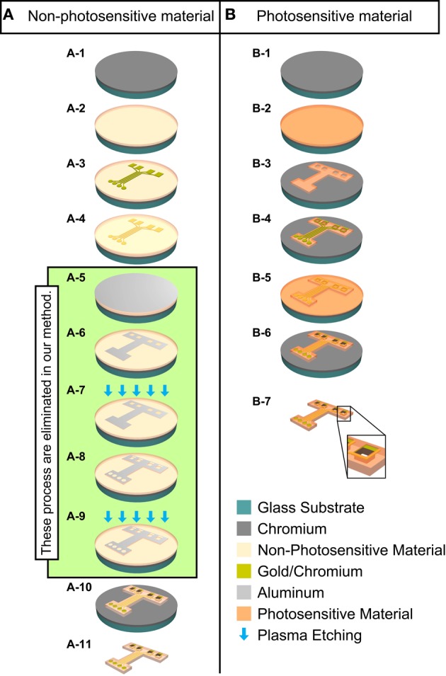
Figure 1.

Schematic diagram of the manufacturing process for the ECoG electrode with MEMS surface-micromachining technologies. Column (A): Conventional fabrication method for non-photosensitive material (non-PSM). Column (B): Fabrication method in this study for photosensitive material (PSM). Dry etching process is green color area from (A-5) to (A-9). (A-1) Cr is deposited on glass on substrate. (A-2) Non-PSM is deposited. (A-3) Chromium/gold is deposited and the recording microelectrodes and hard wiring are patterned. (A-4) Non-PSM is deposited again. (A-5) Aluminum is deposited as a mask for plasma etching. (A-6) Aluminum mask is patterned for the outer geometry and the through-holes of the ECoG electrode. (A-7) Non-PSM is patterned to define the outer geometry and the through-holes of the ECoG electrode by plasma etching. (A-8) Aluminum mask is patterned for the outer geometry, the exposed recording microelectrode sites, and the through-holes by plasma etching. (A-9) Non-PSM is patterned to expose the outer geometry, the exposed recording microelectrode sites, and the through-holes by plasma etching. (A-10) Aluminum is removed. (A-11) The ECoG electrode is lifted off. (B-1) Cr is deposited on glass on substrate. (B-2) PSM is deposited on substrate. (B-3) PSM is patterned to define the outer geometry and the through-holes of the ECoG electrode. (B-4) Chromium/gold is deposited and the recording microelectrodes and hard wiring are patterned. (B-5) PSM is deposited again. (B-6) The outer geometry, the exposed recording microelectrode sites, and the through-holes of the ECoG electrode are patterned. (B-7) The ECoG electrode is lifted off. Large box at the bottom is a magnified illustration of a through-hole.
