Abstract
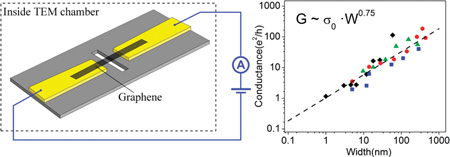
We report electronic measurements on high-quality graphene nanoconstrictions (GNCs) fabricated in a transmission electron microscope (TEM), and the first measurements on GNC conductance with an accurate measurement of constriction width down to 1 nm. To create the GNCs, freely suspended graphene ribbons were fabricated using few-layer graphene grown by chemical vapor deposition. The ribbons were loaded into the TEM, and a current-annealing procedure was used to clean the material and improve its electronic characteristics. The TEM beam was then used to sculpt GNCs to a series of desired widths in the range 1–700 nm; after each sculpting step, the sample was imaged by TEM and its electronic properties were measured in situ. GNC conductance was found to be remarkably high, comparable to that of exfoliated graphene samples of similar size. The GNC conductance varied with width approximately as G(w) = (e2/h)w0.75, where w is the constriction width in nanometers. GNCs support current densities greater than 120 µA/nm2, 2 orders of magnitude higher than that which has been previously reported for graphene nanoribbons and 2000 times higher than that reported for copper.
Keywords: Graphene, electronic transport properties, transmission electron microscopy, graphene nanoribbon, nanofabrication, graphene point contact
Graphene1,2 is a unique material that may soon find use in electronic,3–5 biological,6–8 and optoelectronic4,9,10 applications. However, the production of large-scale, high-quality graphene for electronic devices remains an important challenge. To date, high mobility graphene devices have been primarily fabricated using mechanically exfoliated graphene flakes,11,12 a technique that requires time-intensive characterization procedures13 and is not scalable. Large-scale graphene production methods, such as chemical vapor deposition (CVD) on polycrystalline Cu foil, may be used to create wafer-scale graphene;14 however the reported mobility of the material to date is at least 1 order of magnitude lower than that of exfoliated graphene.14–17 Methods for production of large-area graphene with high mobility are needed in order for electronic applications of graphene to be realized.
Bulk graphene also lacks an energy band gap, making it unsuitable for digital logic applications. A band gap can be engineered into the material by fashioning it into nanoribbons,18–20 nanoconstrictions,21 and quantum dots,22 which are predicted to develop energy gaps due to quantum confinement. The value of the energy gap is modified by edge effects23–25 that are predicted to depend on atomic-scale details of the edge geometry. This motivates the development of techniques for measuring the electronic properties of graphene nanostructures whose structure may also be imaged with subnanometer resolution.
To address these issues, we developed the use of electron beam “nanosculpting” to fabricate graphene nanoconstrictions (GNCs) inside a TEM and measure their widths and electronic properties in situ. Compared to earlier reports based on scanning electron microscopy21 and atomic force microscopy,18,26 our TEM-based approach enables superior control and accurate measurement of the GNC width across a very wide range (1–1000 nm). Current annealing is used to clean the graphene and improve its electronic properties. On the basis of measurements of the resistance of multiple GNCs sculpted from a single nanoribbon, we infer both the contact resistance and the intrinsic conductance of the GNC as a function of its width, information that was not accessible in the earlier experiments. We find that the intrinsic GNC conductance varies with the channel width w approximately as w0.75 over the range 1–700 nm, indicating that the GNCs experience carrier doping so the chemical potential is well away from the charge neutrality point. Current-annealed GNCs have high conductance that is comparable to that of exfoliated graphene samples with similar dimensions, and they withstand a current density of at least 120 µA/nm2, 2 orders of magnitude larger than has been reported previously on graphene nanoribbons.26,27 This work thus provides more understanding of the correlation between graphene structure and performance, and it opens a route toward the study of the effect of atomic-scale edge geometry on the transport properties of graphene nanostructures.
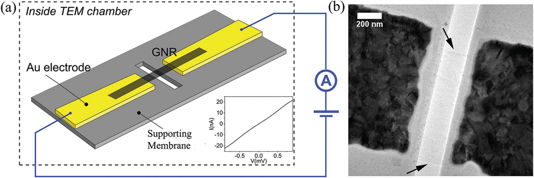
The experiments were based on suspended graphene ribbons on electron-transparent SiN membranes, shown schematically in Figure 1a. Device fabrication began by micromachining a 40 × 40 µm2, 100 nm thick, freely suspended SiN membrane, supported by a bulk silicon wafer.28 A combination of photolithography and electron beam lithography was used to define Au source and drain electrodes with separations of 200 nm to 1 µm, followed by focused ion beam milling to cut a 1.4 µm × 200 nm slit in the SiN membrane in the region between the electrodes. CVD-grown few layer graphene (FLG), ~3–10 layers thick, was transferred to the chip surface17,29 and patterned using electron-beam lithography on negative-tone resist (XR-1541, Dow Corning) and an oxygen plasma etch. This resulted in FLG nanoribbons (typically 3 µm long by 400–800 nm wide) with a small freely suspended region over a slit in the SiN membrane, in good electrical contact with the Au electrodes. The negative-tone resist was removed with a buffered oxide etch immediately before inserting the chip into the TEM on a home-built sample holder with electrical feedthroughs.
Figure 1.
Suspended graphene devices. (a) Sample schematic. Few layer graphene ribbon (3–10 layers thick) is suspended over a 1.4 µm × 0.2 µmslit in a 100 nm thick silicon nitride (SiN) membrane (membrane size ~40 µm × 40 µm). Inset: current–voltage characteristic of an as-fabricated nanoribbon, acquired in situ. (b) TEM image of a suspended graphene nanoribbon. Arrows indicate the edges of the graphene.
Bright field imaging and electrical measurements were performed at room temperature in a JEOL 2010F TEM. An image of a typical suspended FLG nanoribbon is shown in Figure 1b. Two arrows indicate the edges of the material, which is quite faint in this image because it is only a few layers thick. The current–voltage (I–V) characteristic, measured in situ, is shown in the inset of Figure 1a. The initial resistance values of the nanoribbons used in these experiments were in the range 20–200 kΩ.
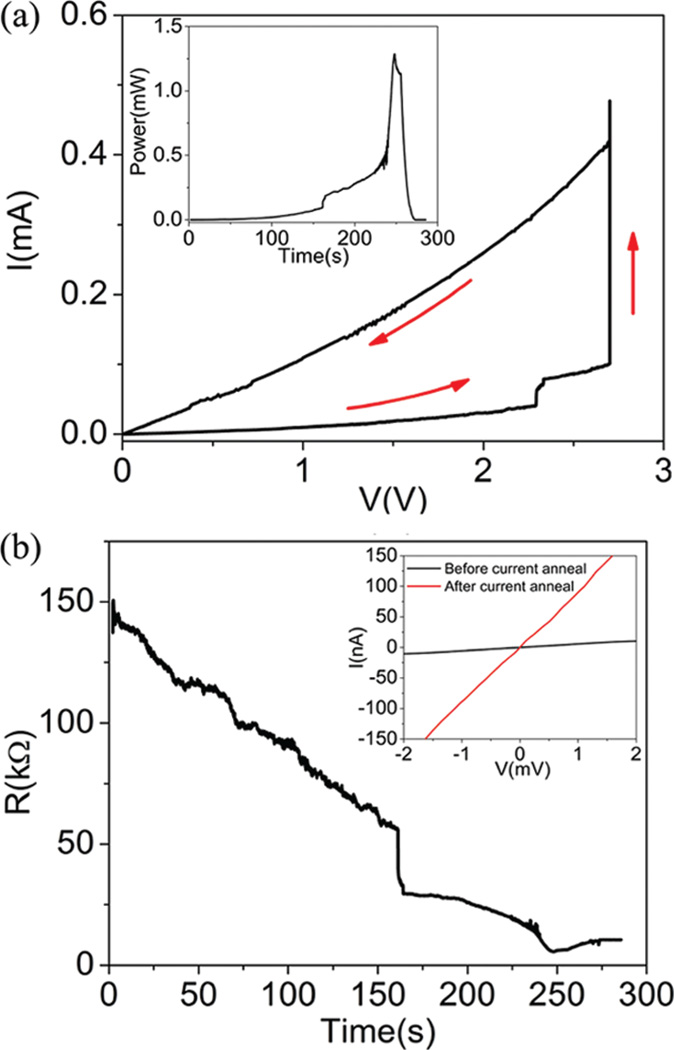
A current annealing (Joule heating) procedure with a slow voltage ramp (~10 mV/s) was performed on the nanoribbon inside the TEM; a typical I–V characteristic for the annealing process is shown in Figure 2a, where red arrows indicate the sweep direction. The Joule power as a function of time is given in the inset of Figure 2a. The maximum dissipated power exceeds 1.2 mW, which is expected to cause the suspended nanoribbon to reach a temperature as high as 2000 °C;30 the high vacuum environment of the TEM chamber (~10 µTorr) prevents oxidation of the FLG.30,31 We observe that the I–V is smooth for V < 2 V, with pronounced current jumps occurring at higher bias (i.e., small and large current jumps at 2.3 and 2.7 V, respectively, in Figure 2a).30 After the annealing process, the I–V characteristic is permanently altered, as evidenced by the hysteresis in Figure 2a.
Figure 2.
Current annealing of graphene devices inside the TEM. (a) Current–voltage (I–V) trace of a graphene ribbon device during current annealing; red arrows show current trace direction as the voltage is increased at a rate of 10 mV/s. Inset: corresponding plot of power vs time. (b) Time evolution of the resistance (R = V/I) of graphene nanoribbon during current annealing. Inset: low bias I–V curve of the same device before and after current annealing.
The evolution of the two-terminal resistance (R = V/I) for the device during current annealing is plotted in Figure 2b. Annealing results in a decrease in device resistance by more than an order of magnitude, from~150 to ~10 kΩ. This is evident in the data of Figure 2b (taken at variable, relatively high bias voltage), as well as the low-voltage I–V characteristics measured before and after annealing (inset to Figure 2b).
We attribute the current jumps and significant decrease in resistance that occur during current annealing to three factors. First, Joule heating of the sample to ~300–400 °C is expected to cause vaporization of resist residue from the lithography processes and an associated increase in carrier mobility.32,33 This temperature range is consistent with an applied voltage of 2.3 V, where the smaller current jump is observed in Figure 2a. TEM images of FLG nanoribbons taken before and after annealing clearly indicate contamination removal as impurities evaporate from the surface (see Figure S1 in the Supporting Information). Second, high-temperature annealing has been shown to reduce the contact resistance between metal electrodes and carbon nanomaterials.34 Finally, we observe that high-temperature current annealing induces a structural reconfiguration and recrystallization of the FLG ribbon, as observed by others30,31 and discussed in the Supporting Information. Current annealing thus significantly improves the structural and electronic properties of the CVD graphene.
After current annealing, nanosculpting with the focused electron beam35 was used to define nanoconstrictions (GNCs) from the suspended ribbon. Beam irradiation was used to knock out carbon atoms from the ribbon edges and in this way gradually reduce the ribbon width. In order to nanosculpt the ribbon, the TEM magnification was increased to ~800000×, the electron beam was focused to its minimum diameter, ~1 nm, and the beam was moved with the condenser deflectors to expose and remove graphene at a rate of ~1 nm2/s.
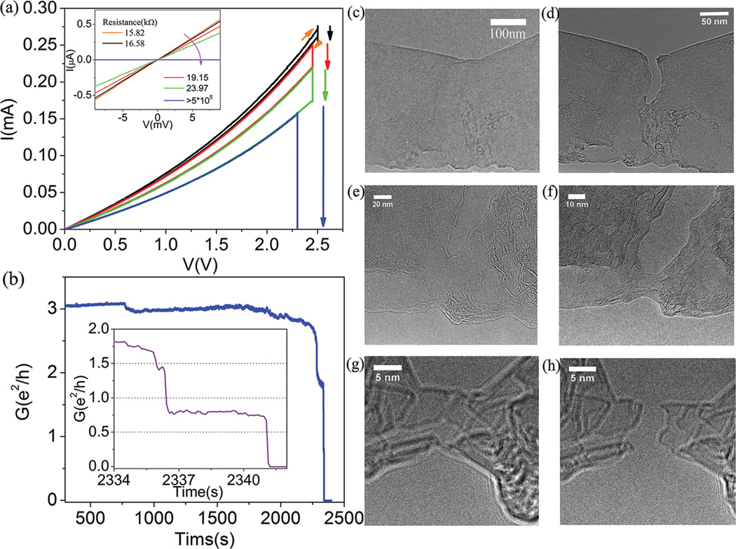
Nanosculpting was performed with an applied electrical bias voltage to heat the sample, which suppresses deposition of amorphous carbon31 and damage of the lattice by the electron beam.36,37 Figure 3a shows I–V traces taken during a set of four nanosculpting steps, where a nanoribbon was progressively narrowed from 280 to 14 nm to yield GNCs of different widths. To begin nanosculpting, the bias voltage was ramped to ~2.3 V and the current allowed to stabilize. The focused TEM beam was used to remove graphene from the sample edge, leading to a current decrease (vertical arrow). After each sculpting step, the low-bias I–V characteristic was measured with the TEM beam off to prevent carbon deposition (inset to Figure 3a) and the GNC was imaged (Figure 3c–f). Data correlating GNC width and electrical resistance from multiple samples are analyzed below.
Figure 3.
TEM in situ fabrication of graphene nanoconstriction. (a) Current–voltage (I–V) traces of graphene nanoconstriction during fabrication using electron beam sculpting. Black, red, blue, and green curves are I–V curves after four subsequent sculpting steps to reduce the constriction width, and vertical arrows indicate the associated conductance drops. Orange arrows on the black trace indicate direction of the voltage sweep. (Inset) Low bias I–V curves measured after each sculpting step. (b) Conductance vs time plot of graphene constriction between the end of the last sculpting step (w = 5 nm) and spontaneous breaking of the constriction (w = 0 nm) under voltage bias, where the contact resistance has been subtracted. Inset shows conductance vs time over the last 8 s. (c–h) TEM images for the same GNCs after each subsequent sculpting step from a width of (w = 280 nm) to fully broken (w = 0 nm). Note that (g) and (h) were taken at a slightly different focal point to enhance the contrast of the very thin GNCs.
The width of the sample in Figure 3 was reduced to 5 nm by a final nanosculpting step, and the device was allowed to break under the stress of the applied voltage (Figure 3g–h). Figure 3b shows the time evolution of the device conductance from a value of ~3 e2/h to zero when the nanoconstriction breaks (the contact resistance has been subtracted off, as described below). The inset to Figure 3b is a higher resolution view of how the device conductance evolves during the last few seconds before the constriction fails. In contrast to the breaking of metallic junctions, where atom-by-atom removal leads to quantized steps in the conductance,38 GNCs break in a less controlled way, consistent with the existence of strong covalent bonds between the carbon atoms. Junctions often break when they are several carbon atoms wide (e.g., Figure 3g–h), and the conductance value immediately before the break shows significant device-to-device variation.
The TEM nanosculpting procedure enabled reliable fabrication and inspection of GNCs with arbitrary widths as small as 1 nm. Electronic measurements taken during and after the sculpting procedure provided correlated data on GNC conductance and current density as a function of GNC width. For the device highlighted in Figure (3), we estimate the GNC thickness of two layers (0.6 nm) and a final width of 5 ± 0.5 nm at its narrowest point, implying that this particular GNC supported a current density in excess of 30 µA/nm2. The other GNC samples measured during this work supported current densities of 20–120 µA/nm2 without failure, 2 orders of magnitude higher than that which has been previously reported for graphene nanoribbons27,39 and ~2000 times higher than that for copper.
We attribute the high current density to several factors. First, we expect that current annealing leads to improved quality of the FLG material. This assumption is supported by the observation that GNC conductance is comparable to that found for samples we created by mechanical exfoliation. For example, we measure a conductance of 500 µS (1300 µS) for a 20 nm wide (50 nm wide) GNC, and we use data from an earlier report19 and find a value of 750 µS (2000 µS) for exfoliated samples of similar length and width. Second, we assume that our GNCs are shorter than the mean free path for phonon scattering and therefore support quasi-ballistic electron transport, with most of the dissipation occurring in the bulk leads rather than the GNC; this phenomenon will lead to enhanced current carrying capacity, as is known to occur for carbon nanotubes.40 Finally, based on Figure 3g and similar images (see Supporting Information), we expect that current annealed GNCs have crystallographically oriented edges (for example, zigzag edges), which sharply reduces edge scattering and enhances conduction. It is also possible that stable nanotube structures form in the narrowest GNCs,31 providing an additional conduction channel and increased current density. Future work with an aberration-corrected TEM will provide more definitive structural information on the GNCs and enable comparison of the measurements with experimental41 and computational42 work on graphene quantum point contacts.
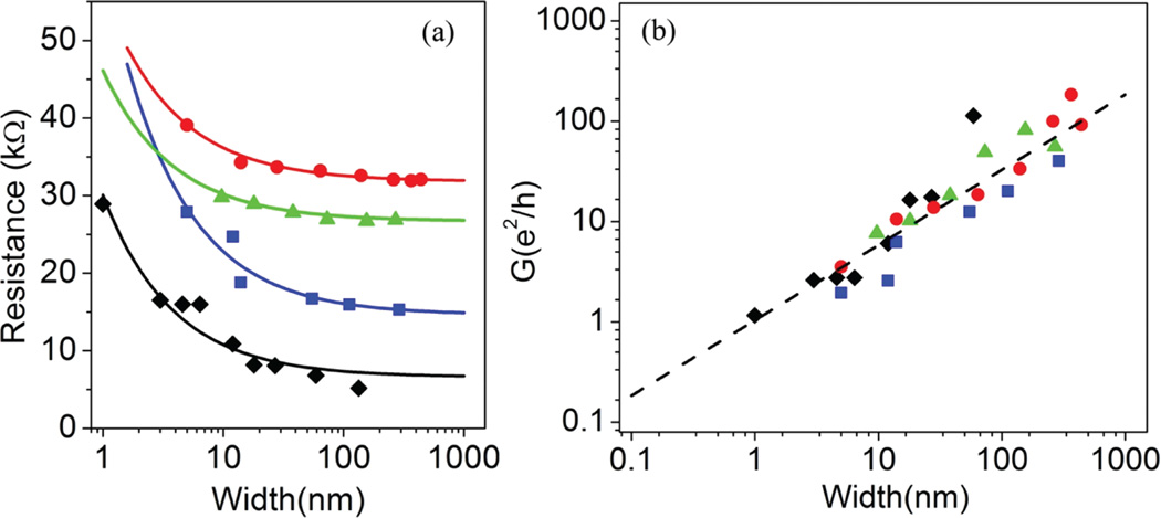
Figure 4a shows two-terminal resistance, RTOT, as a function of width for four sets of GNCs, each fabricated from a suspended nanoribbon samples using the TEM nanosculpting process outlined above. For each GNC set, we fit the data with the form RTOT = RC + RMw−α, where w is the measured width of the GNC (in nanometers), and the contact resistance, RC, RM (with units of resistance), and α are fitting parameters. The contact resistance is expected to include contributions from the wiring, the gold–graphene contact interface, and wide graphene regions outside of the GNC. Although a natural expectation for the power law parameter is α = 1, appropriate for an Ohmic conductor, this value provides a consistently poor fit to the data, with unphysical values for the contact resistance (see Supporting Information for details). We find far superior fits to the data for α = 0.75, as illustrated in Figure 4a.
Figure 4.
Resistance and conductance as a function of device width. (a) Two-terminal GNC resistance as a function of width. Blue, green, and red data are offset from each other by 10 kΩ for clarity; error bars are smaller than the symbol size. Fits are of the form RTOT = RC + RMw−α with α = 0.75 and w, the GNC width measured in nanometers: black fit, RC = 6.6 kΩ, RM = 23 kΩ; blue fit, RC = 4.6 kΩ, and RM = 46 kΩ; greenfit, RC = 6.4 kΩ and RM = 19 kΩ; red fit, RC = 1.8 kΩ and RM = 24 kΩ. (b) GNC conductance as a function of width with the contact resistance subtracted. Dashed line is a fit of the form G ~ σ0wα with α = 0.75, w is the width of the GNC in nm, and σ0 = e2/h (R2 value of 0.86).
Figure 4(b) shows conductance versus width for all the GNC data, after removal of the best-fit contact resistance, RC. The full data set is well fit over its entire range by the functional formG= σ0w0.75, where σ0 = e2/h, and w is GNC width measured in nanometers. Choices of the power law parameter outside the range α = 0.7 – 0.8 lead to fits of significantly lower quality (see Supporting Information).
This is a surprising observation in several ways. First, as mentioned earlier, we expect the confinement to induce an energy gap in the material, but there is little evidence of this in the data, where very high conductance is observed for the GNC down to a width of 1 nm. This observation is consistent with the presence of unintentional carrier doping such that the chemical potential for the system lies outside the energy gap. It is notable that the confinement-induced energy gap of a bare (unterminated) graphene nanoribbon is computed to vary as Eg ~ w−b, with the power law b in the range 0.75–0.9.24,25 To reconcile this scaling with our finding that G ~ w0.75, we would need to assume that Eg ~ 1/w. However, we are not aware of an established relationship between the energy gap and the conductance at large Fermi energy. Second, contrast changes observed in TEM images of GNCs (panels c–h of Figure 3 and especially panel f)) indicate the material becomes thinner as it is narrowed by nanosculpting. On the baisis of the quality of the power law fit even as the GNC thickness varies, we conclude that the bulk of the conduction is carried by only a few (1 or 2) of the graphene layers that comprise the GNC, which are recrystallized by the annealing process (see Supporting Information), and perhaps thermally bonded to the Au electrodes. The TEM fabrication and measurement capability introduced here will enable future experiments to clarify these issues.
In summary, we have presented a robust methodology for the fabrication and in situ measurement of graphene nanoconstrictions inside a TEM. GNCs formed by nanosculpting have high conductance comparable to that of exfoliated graphene, and they are able to sustain current densities in excess of 100 µA/nm2. We measured the electrical properties of GNCs with widths in the range 1–1000 nm and found that the GNC conductance varies approximately as w0.75. Future work, including the use of an aberration-corrected TEM to allow for single-atom resolution imaging, may further illuminate the properties of GNCs and enable correlation of the sample conductance with the precise edge structure.
Supplementary Material
ACKNOWLEDGMENT
The authors thank Dr. Zhengtang Luo for useful discussions and development of the CVD graphene growth process used in these experiments and Drs. Julio Rodriguez-Manzo and Branislav Nikolic for comments on the manuscript. This work was supported by the National Science Foundation through Grant #DMR-0805136 (Y.L. and A.T.C.J.) and NIH Grant R21HG 004767 and R21HG 557611 (C.M. and M.D.). Use of facilities of the Nano/Bio Interface Center is gratefully acknowledged.
Footnotes
ASSOCIATED CONTENT
Supporting Information. Additional TEM images of a sample before and after in situ current annealing, a control experiment to study the effects of carbon contamination, TEM images of two GNCs of width 6 and 1 nm, and further analysis of data in Figure 4b. This material is available free of charge via the Internet at http://pubs.acs.org.
REFERENCES
- 1.Novoselov KS, Geim AK, Morozov SV, Jiang D, Katsnelson MI, Grigorieva IV, Dubonos SV, Firsov AA. Nature. 2005;438:197–200. doi: 10.1038/nature04233. [DOI] [PubMed] [Google Scholar]
- 2.Geim AK, Novoselov KS. Nat. Mater. 2007;6:183–191. doi: 10.1038/nmat1849. [DOI] [PubMed] [Google Scholar]
- 3.Wu Y, Lin Y-m, Bol AA, Jenkins KA, Xia F, Farmer DB, Zhu Y, Avouris P. Nature. 2011;472:74–78. doi: 10.1038/nature09979. [DOI] [PubMed] [Google Scholar]
- 4.Bae S, Kim H, Lee Y, Xu X, Park J-S, Zheng Y, Balakrishnan J, Lei T, Ri Kim H, Song YI, Kim Y-J, Kim KS, Ozyilmaz B, Ahn J-H, Hong BH, Iijima S. Nat. Nanotechnol. 2010;5:574–578. doi: 10.1038/nnano.2010.132. [DOI] [PubMed] [Google Scholar]
- 5.Lu Y, Goldsmith BR, Kybert NJ, Johnson ATC. Appl. Phys. Lett. 2010;97 083107. [Google Scholar]
- 6.Merchant C, Healey K, Wanunu M, Ray V, Peterman N, Bartel J, Fischbein M, Venta K, Luo Z, Johnson ATC, Drndić M. Nano Lett. 2010;10:2915–2921. doi: 10.1021/nl101046t. [DOI] [PubMed] [Google Scholar]
- 7.Schneider GgF, Kowalczyk SW, Calado VE, Pandraud Gg, Zandbergen HW, Vandersypen LMK, Dekker C. Nano Lett. 2010;10:3163–3167. doi: 10.1021/nl102069z. [DOI] [PubMed] [Google Scholar]
- 8.Garaj S, Hubbard W, Reina A, Kong J, Branton D, Golovchenko JA. Nature. 2010;467:190–193. doi: 10.1038/nature09379. [DOI] [PMC free article] [PubMed] [Google Scholar]
- 9.Li X, Zhu Y, Cai W, Borysiak M, Han B, Chen D, Piner RD, Colombo L, Ruoff RS. Nano Lett. 2009;9:4359–4363. doi: 10.1021/nl902623y. [DOI] [PubMed] [Google Scholar]
- 10.Xia F, Mueller T, Lin Y-m, Valdes-Garcia A, Avouris P. Nat. Nanotechnol. 2009;4:839–843. doi: 10.1038/nnano.2009.292. [DOI] [PubMed] [Google Scholar]
- 11.Bolotin KI, Sikes KJ, Jiang Z, Klima M, Fudenberg G, Hone J, Kim P, Stormer HL. Solid State Commun. 2008;146:351–355. [Google Scholar]
- 12.Chen JH, Jang C, Xiao SD, Ishigami M, Fuhrer MS. Nat. Nanotechnol. 2008;3:206–209. doi: 10.1038/nnano.2008.58. [DOI] [PubMed] [Google Scholar]
- 13.Novoselov KS, Geim AK, Morozov SV, Jiang D, Zhang Y, Dubonos SV, Grigorieva IV, Firsov AA. Science. 2004;306:666–669. doi: 10.1126/science.1102896. [DOI] [PubMed] [Google Scholar]
- 14.Li X, Cai W, An J, Kim S, Nah J, Yang D, Piner R, Velamakanni A, Jung I, Tutuc E, Banerjee SK, Colombo L, Ruoff RS. Science. 2009;324:1312–1314. doi: 10.1126/science.1171245. [DOI] [PubMed] [Google Scholar]
- 15.Bae S, Kim H, Lee Y, Xu X, Park J-S, Zheng Y, Balakrishnan J, Lei T, Ri Kim H, Song YI, Kim Y-J, Kim KS, Ozyilmaz B, Ahn J-H, Hong BH, Iijima S. Nat Nano. 2010;5:574–578. doi: 10.1038/nnano.2010.132. [DOI] [PubMed] [Google Scholar]
- 16.Cao H, Yu Q, Jauregui LA, Tian J, Wu W, Liu Z, Jalilian R, Benjamin DK, Jiang Z, Bao J, Pei SS, Chen YP. Appl. Phys. Lett. 2010;96 122106–3. [Google Scholar]
- 17.Luo Z, Lu Y, Singer DW, Berck ME, Somers LA, Goldsmith BR, Johnson ATC. Chem. Mater. 2011;23:1441–1447. [Google Scholar]
- 18.Li X, Wang X, Zhang L, Lee S, Dai H. Science. 2008;319:1229–1232. doi: 10.1126/science.1150878. [DOI] [PubMed] [Google Scholar]
- 19.Han MY, Ozyilmaz B, Zhang Y, Kim P. Phys. Rev. Lett. 2007;98:206805. doi: 10.1103/PhysRevLett.98.206805. [DOI] [PubMed] [Google Scholar]
- 20.Tapaszto L, Dobrik G, Lambin P, Biro LP. Nat. Nanotechnol. 2008;3:397–401. doi: 10.1038/nnano.2008.149. [DOI] [PubMed] [Google Scholar]
- 21.Lu Y, Goldsmith B, Strachan DR, Lim JH, Luo Z, Johnson ATC. Small. 2010;6:2748–2754. doi: 10.1002/smll.201001324. [DOI] [PubMed] [Google Scholar]
- 22.Ponomarenko LA, Schedin F, Katsnelson MI, Yang R, Hill EW, Novoselov KS, Geim AK. Science. 2008;320:356–358. doi: 10.1126/science.1154663. [DOI] [PubMed] [Google Scholar]
- 23.Nakada K, Fujita M, Dresselhaus G, Dresselhaus MS. Phys. Rev. B. 1996;54:17954–17961. doi: 10.1103/physrevb.54.17954. [DOI] [PubMed] [Google Scholar]
- 24.Son Y-W, Cohen ML, Louie SG. Phys. Rev. Lett. 2006;97:216803. doi: 10.1103/PhysRevLett.97.216803. [DOI] [PubMed] [Google Scholar]
- 25.Barone V, Hod O, Scuseria GE. Nano Lett. 2006;6:2748–2754. doi: 10.1021/nl0617033. [DOI] [PubMed] [Google Scholar]
- 26.Wang X. Phys. Rev. Lett. 2008;100:206803. doi: 10.1103/PhysRevLett.100.206803. [DOI] [PubMed] [Google Scholar]
- 27.Kim K, Sussman A, Zettl A. ACS Nano. 2010;4:1362–1366. doi: 10.1021/nn901782g. [DOI] [PubMed] [Google Scholar]
- 28.Strachan DR, Johnston DE, Guiton BS, Datta SS, Davies PK, Bonnell DA, Johnson AT. Phys. Rev. Lett. 2008;100 doi: 10.1103/PhysRevLett.100.056805. 056805. [DOI] [PubMed] [Google Scholar]
- 29.Merchant CA, Healy K, Wanunu M, Ray V, Peterman N, Bartel J, Fischbein MD, Venta K, Luo Z, Johnson ATC, Drndić M. Nano Lett. 2010;10:2915–2921. doi: 10.1021/nl101046t. [DOI] [PubMed] [Google Scholar]
- 30.Jia X, Hofmann M, Meunier V, Sumpter BG, Campos-Delgado J, Romo-Herrera JM, Son H, Hsieh Y-P, Reina A, Kong J, Terrones M, Dresselhaus MS. Science. 2009;323:1701–1705. doi: 10.1126/science.1166862. [DOI] [PubMed] [Google Scholar]
- 31.Song B, Schneider GF, Xu Q, Pandraud G, Dekker C, Zandbergen H. Nano Lett. 2011;11:2247–2250. doi: 10.1021/nl200369r. [DOI] [PubMed] [Google Scholar]
- 32.Dan Y, Lu Y, Kybert NJ, Luo Z, Johnson ATC. Nano Lett. 2009;9:1472–1475. doi: 10.1021/nl8033637. [DOI] [PubMed] [Google Scholar]
- 33.Moser J, Barreiro A, Bachtold A. Appl. Phys. Lett. 2007;91:163513. [Google Scholar]
- 34.Kane AA, Sheps T, Branigan ET, Apkarian VA, Cheng MH, Hemminger JC, Hunt SR, Collins PG. Nano Lett. 2009;9:3586–3591. doi: 10.1021/nl9017995. [DOI] [PubMed] [Google Scholar]
- 35.Fischbein MD, Drndic M. Appl. Phys. Lett. 2008;93 113107–3. [Google Scholar]
- 36.Krasheninnikov AV, Banhart F. Nat. Mater. 2007;6:723–733. doi: 10.1038/nmat1996. [DOI] [PubMed] [Google Scholar]
- 37.Huang JY, Chen S, Ren ZF, Chen G, Dresselhaus MS. Nano Lett. 2006;6:1699–1705. doi: 10.1021/nl0609910. [DOI] [PubMed] [Google Scholar]
- 38.Strachan DR, Smith DE, Fischbein MD, Johnston DE, Guiton BS, Drndic M, Bonnell DA, Johnson AT. Nano Lett. 2006;6:441–444. doi: 10.1021/nl052302a. [DOI] [PubMed] [Google Scholar]
- 39.Lomeda JR, Doyle CD, Kosynkin DV, Hwang W-F, Tour JM. J. Am. Chem. Soc. 2008;130:16201–16206. doi: 10.1021/ja806499w. [DOI] [PubMed] [Google Scholar]
- 40.Javey A, Guo J, Paulsson M, Wang Q, Mann D, Lundstrom M, Dai HJ. Phys. Rev. Lett. 2004;92 doi: 10.1103/PhysRevLett.92.106804. -. [DOI] [PubMed] [Google Scholar]
- 41.Nakaharai S, Williams JR, Marcus CM. Phys. Rev. Lett. 2011;107 doi: 10.1103/PhysRevLett.107.036602. 036602. [DOI] [PubMed] [Google Scholar]
- 42.Erdogan E, Popov I, Seifert G. Phys. Rev. B. 2011;83:245417. [Google Scholar]
- 43.Son YW, Cohen ML, Louie SG. Phys. Rev. Lett. 2006;97:216803. doi: 10.1103/PhysRevLett.97.216803. [DOI] [PubMed] [Google Scholar]
Associated Data
This section collects any data citations, data availability statements, or supplementary materials included in this article.


