
Fig. 1.
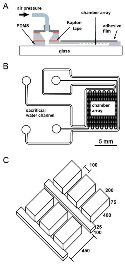
Design of the digital LAMP self-digitization chip. (A) Schematic diagram showing the individual components of a fully assembled chip. The drawing is not to scale. The microfluidic array was embedded in a thin piece of PDMS, which was covered by a sealant film on top and a PDMS coated cover slip on the bottom. Air pressure was delivered via a removable adapter, which was connected to an external pressure source. (B) Layout of the microfluidic network. A dense array of rectangular side chambers was connected to a thin main channel. The whole array was surrounded by a separate water reservoir to saturate the PDMS during incubation at 65 °C. The scale bar represents 5 mm. (C) Geometry of the side chamber array and main channel. All dimensions are in micrometers.