
Figure 4.
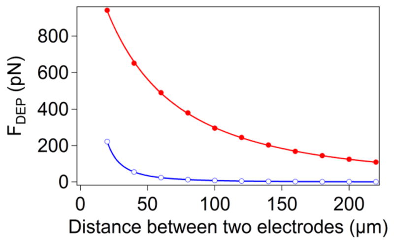
Simulation results of DEP force as a function of the electrode separation for probes placed 50 nm above the surface of a flat substrate (○), Geometry A, or the bottom of the microwell (●), Geometry C. The parameters used for the simulation were 10 V peak-to-peak voltage with a 3 μm diameter probe. The curves represent the power law FDEP ∝ 1/sn for a Geometry A, where n=1.987±0.001, and the square of a function in Eq. 6 for a Geometry B.